Pixel Sizes and Optics
Understanding the interplay between camera sensors and imaging lenses is a vital part of designing and implementing a machine vision system. The optimization of this relationship is often overlooked, and the impact that it can have on the overall resolution of the system is large. An improperly paired camera/lens combination could lead to wasted money on the imaging system. Unfortunay, determining which lens and camera to use in any application is not always an easy task: more camera sensors (and as a direct result, more lenses) continue to be designed and manufactured to take advantage of new manufacturing capabilities and drive performance up. These new sensors present a number of challenges for lenses to overcome, and make the correct camera to lens pairing less obvious.
The first challenge is that pixels continue to get smaller. While smaller pixels typically mean higher system-level resolution, this is not always the case once the optics utilized are taken into account. In a perfect world, with no diffraction or optical errors in a system, resolution would be based simply upon the size of a pixel and the size of the object that is being viewed (see our application noteObject Space Resolution for further explanation). To briefly summarize, as pixel size decreases, the resolution increases. This increase occurs as smaller objects can be fit onto smaller pixels and still be able to resolve the spacing between the objects, even as that spacing decreases. This is an oversimplified model of how a camera sensor detects objects, not taking noise or other parameters into account.
Lenses also have resolution specifications, but the basics are not quite as easy to understand as sensors since there is nothing quite as concrete as a pixel. However, there are two factors that ultimay determine the contrast reproduction (modulation transfer function, or MTF) of a particular object feature onto a pixel when imaged through a lens: diffraction and aberrational content. Diffraction will occur anytime light passes through an aperture, causing contrast reduction (more details in our application noimitations on Resolution and Contrast: The Airy Disk). Aberrations are errors that occur in every imaging lens that either blur or misplace image information depending on the type of aberration (more information on individual optical aberrations can be found in our application note How Aberrations Affect Machine Vision Lenses. With a fast lens (≤f/4), optical aberrations are most often the cause for a system departing from “perfect” as would be dictated by the diffraction limit; in most cases, lenses simply do not function at their theoretical cutoff frequency (ξCutoff), as dictated by Equation 1.
To relate this equation back to a camera sensor, as the frequency of pixels increases (pixel size goes down), contrast goes down - every lens will always follow this trend. However, this does not account for the real world hardware performance of a lens. How tightly a lens is toleranced and manufactured will also have an impact on the aberrational content of a lens and the real-world performance will differ from the nominal, as-designed performance. It can be difficult to approximate how a real world lens will perform based on nominal data, but tests in a lab can help determine if a particular lens and camera sensor are compatible.
One way to understand how a lens will perform with a certain sensor is to test its resolution with a USAF 1951 bar target. Bar targets are better for determining lens/sensor compatibility than star targets, as their features line up better with square (and rectangular) pixels. The following examples show test images taken with the same high resolution 50mm focal length lens and the same lighting conditions on three different camera sensors. Each image is then compared to the lens’s nominal, on-axis MTF curve (blue curve). Only the on-axis curve is used in this case because the region of interest where contrast was measured only covered a small portion of the center of the sensor. Figure 1 shows the performance of the 50mm lens when paired with a 1/2.5” ON Semiconductor MT9P031 with 2.2µm pixels, when at a magnification of 0.177X. Using Equation 1 from our application note Resolution, the sensor’s Nyquist resolution is 227.7 lp/mm, meaning that the smallest object that the system could theoretically image when at a magnification of 0.177X is 12.4µm (using an alternate form of Equation 7 from our application note Resolution).

Keep in mind that these calculations have no contrast value associated with them. The left side of Figure 1 shows the images of two elements on a USAF 1951 target; the image shows two pixels per feature, and the bottom image shows one pixel per feature. At the Nyquist frequency of the sensor (227 lp/mm), the system images the target with 8.8% contrast, which is below the recommended 20% minimum contrast for a reliable imaging system. Note that by increasing the feature size by a factor of two to 24.8μm, the contrast is increased by nearly a factor of three. In a practical sense, the imaging system would be much more reliable at half the Nyquist frequency.
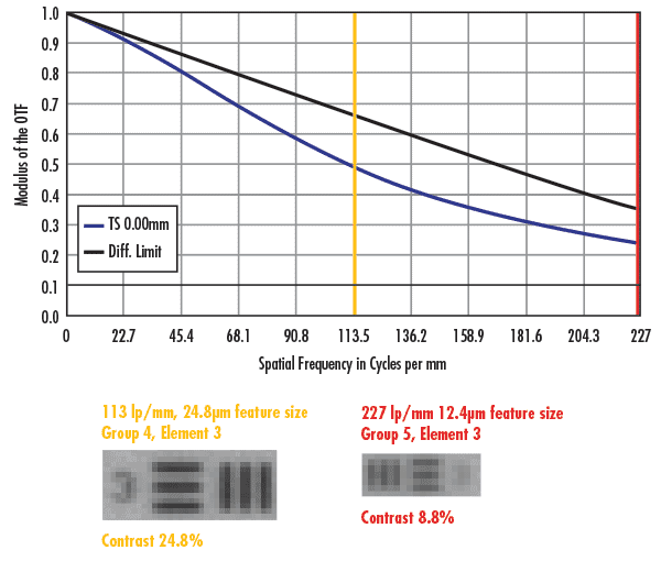
Figure 1: Comparison nominal lens performance vs. real-world performance for a high resolution 50mm lens on the ON Semiconductor MT9P031 with 2.2µm pixels. The red line shows the Nyquist limit of the sensor and the yellow line shows half of the Nyquist limit.
The conclusion that the imaging system could not reliably image an object feature that is 12.4µm in size is in direct opposition to what the equations in our application note Resolution show, as mathematically the objects fall within the capabilities of the system. This contradiction highlights that first order calculations and approximations are not enough to determine whether or not an imaging system can achieve a particular resolution. Additionally, a Nyquist frequency calculation is not a solid metric on which to lay the foundation of the resolution capabilities of a system, and should only be used as a guideline of the limitations that a system will have. A contrast of 8.8% is too low to be considered accurate since minor fluctuations in conditions could easily drive contrast down to unresolvable levels.
Figures 2 and 3 show similar images to those in Figure 1 though the sensors used were the Sony ICX655 (3.45µm pixels) and ON Semiconductor KAI-4021 (7.4µm pixels). The images in each figure show two pixels per feature and the bottom images show one pixel per feature. The major difference between the three Figures is that all of the image contrasts for Figures 2 and 3 are above 20%, meaning (at first glance) that they would be reliable at resolving features of that size. Of course, the minimum sized objects they can resolve are larger when compared to the 2.2µm pixels in Figure 1. However, imaging at the Nyquist frequency is still ill-advised as slight movements in the object could shift the desired feature between two pixels, making the object unresolvable. Note that as the pixel sizes increase from 2.2µm, to 3.45µm, to 7.4µm, the respective increases in contrast from one pixel per feature to two pixels per feature are less impactful. On the ICX655 (3.45µm pixels), the contrast changes by just under a factor of 2; this effect is further diminished with the KAI-4021 (7.4µm pixels).
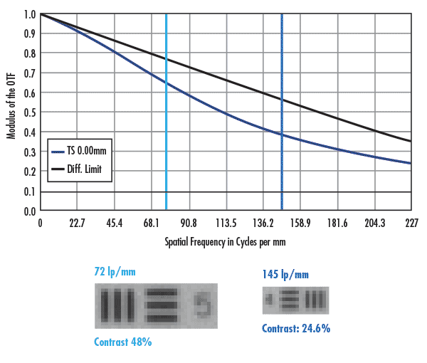
Figure 2: Comparison nominal lens performance vs. real-world performance for a high resolution 50mm lens on the Sony ICX655 with 3.45µm pixels. The dark blue line shows the Nyquist limit of the sensor, and the light blue line shows half of the Nyquist limit.
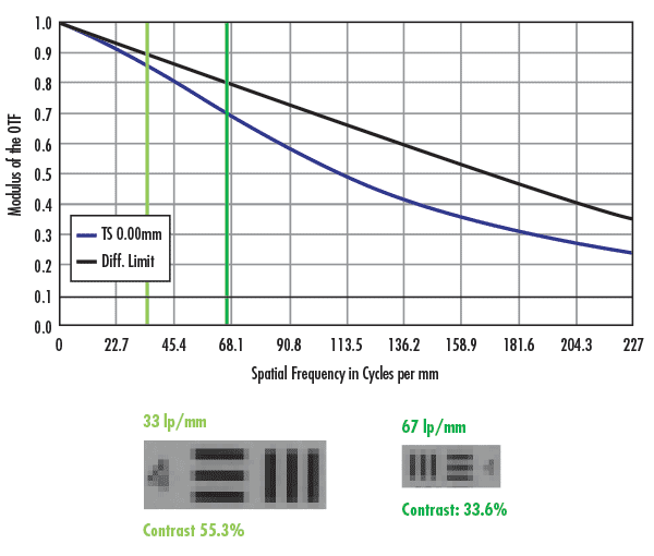
Figure 3: Comparison nominal lens performance vs. real-world performance for a high resolution 50mm lens on the ON Semiconductor KAI-4021 with 7.4µm pixels. The dark green line shows the Nyquist limit of the sensor, and the light green line shows half of the Nyquist limit.
An important discrepancy in Figures 1, 2, and 3 is the difference between the nominal lens MTF and the real-world contrast in an actual image. The MTF curve of the lens on the right side of Figure 1 shows that the lens should achieve approximay 24% contrast at the frequency of 227 lp/mm, when the contrast value produced was 8.8%. There are two main contributors to this difference: sensor MTF and lens tolerances. Most sensor companies do not publish MTF curves for their sensors, but they have the same general shape that the lens has. Since system-level MTF is a product of the MTFs of all of the components of a system, the lens and the sensor MTFs must be multiplied together to provide a more accurate conclusion of the overall resolution capabilities of a system. As mentioned above, a toleranced MTF of a lens is also a departure from the nominal. All of these factors combine to change the expected resolution of a system, and on its own, a lens MTF curve is not an accurate representation of system-level resolution.
As seen in the images in Figure 4, the best system-level contrast is in the images taken with the larger pixels. As the pixel size decreases, the contrast drops considerably. A good best practice is to use 20% as a minimum contrast in a machine vision system, as any contrast value below that is too susceptible to fluctuations in noise coming from temperature variations or crosstalk in illumination. The image taken with the 50mm lens and the 2.2µm pixel in Figure 1 has a contrast of 8.8% and is too low to rely on the image data for object feature sizes corresponding to the 2.2µm pixel size because the lens is on the brink of becoming the limiting factor in the system. Sensors with pixels much smaller than 2.2µm certainly exist and are quite popular, but much below that size becomes nearly impossible for optics to resolve down to the individual pixel level. This means that the equations described in our application note Resolution become functionally meaningless for helping to determine system-level resolution, and images similar to those taken in the aforementioned figures would be impossible to capture. However, these tiny pixels still have a use - just because optics cannot resolve the entire pixel does not render them useless. For certain algorithms, such as blob analysis or optical character recognition (OCR), it is less about whether the lens can actually resolve down to the individual pixel level and more about how many pixels can be placed over a particular feature. With smaller pixels subpixel interpolation can be avoided, which will add to the accuracy of any measurement done with it. Additionally, there is less of a penalty in terms of resolution loss when switching to a color camera with a Bayer pattern filter.
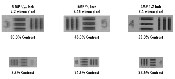
Figure 4: Images taken with the same lens and lighting conditions on three different camera sensors with three different pixel sizes. The images are taken with four pixels per feature, and the bottom images are taken with two pixels per feature.
Another important point to remember is that jumping from one pixel per feature to two pixels per feature gives a substantial amount of contrast back, particularly on the smaller pixels. Although by halving the frequency, the minimum resolvable object effectively doubles in size. If it is absoluy necessary to view down to the single pixel level, it is often better to double the optics’ magnification and halve the field of view. This will cause the feature size to cover twice as many pixels and the contrast will be much higher. The downside to this solution is that less of the overall field will be visible. From the image sensor perspective, the best thing to do is to maintain the pixel size and double the format size of the image sensor. For example, an imaging system with a 1X magnification using a ½” sensor with a 2.2µm pixel will have the same field of view and spatial resolution as a 2X magnification system using a 1” sensor with a 2.2µm pixel, but with the 2X system, the contrast is theoretically doubled.
Unfortunay, doubling the sensor size creates additional problems for lenses. One of the major cost drivers of an imaging lens is the format size for which it was designed. Designing an objective lens for a larger format sensor takes more individual optical components; those components need to be larger and the tolerancing of the system needs to be tighter. Continuing from the example above, a lens designed for a 1” sensor may cost five times as much as a lens designed for a ½” sensor, even if it cannot hit the same pixel limited resolution specifications.
版权所有 © 2026 江阴韵翔光电技术有限公司 备案号:苏ICP备16003332号-1 技术支持:化工仪器网 管理登陆 GoogleSitemap